Charged Device Model (CDM) electrostatic discharge is a common cause of microelectronic circuit failure. Sensitive devices can be seriously damaged or destroyed by a CDM discharge at relatively low voltage. This often occurs when the static charged device contacts a metal surface at a different potential. Such an electrostatic discharge often has an extremely fast rise time.
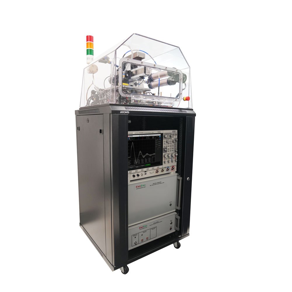
The Model ES640 Charged Device Model (CDM) Test System is a robotic CDM test system designed to meet all popular CDM test methods, allowing both field induced air discharge methods (FICDM) and contact first (CCDM) methods. The system includes a computer, environment-controlled chamber, precision XYZ motion system, different types of CDM test setups, and an automated test and data analysis software.
The Model ES640 Charged Device Model (CDM) Test System is a robotic CDM test system designed to meet all popular CDM test methods, allowing both field induced air discharge methods (FICDM) and contact first (CCDM) methods. The system includes a computer, environment-controlled chamber, precision XYZ motion system, different types of CDM test setups, and an automated test and data analysis software.
| Parameters | ES640-150 | ES640-300 | Unit | Comments |
| Max XY Motion Area | ≥ 150 X 150 | ≥ 300 X 300 | mm | Customizable |
| Max DUT Surface Area | 160 X 160 200 X 300 |
320 X 320 400 X 600 |
mm | Standard Charge Plate Enlarged Charge Plate |
| Max Z Travel Distance | ≥ 50 | mm | Customizable | |
| Min X, Y, Z Step Size | 100 | nm | ||
| Reposition Repeatability | ≤ ±6 | μm | ||
| Test Voltage Range | ± 1 to 2000 or 4000 | V | Default 2000V, Customizable | |
| Test Voltage Step | 1 | V | ||
| Test Voltage Accuracy | ± 1% ± 0.1V | % | ||
| XY Vision Resolution | 1920 X 1080 | Pixel | Zoom & Pan | |
| Vertical Vision Resolution | 2592 X 1944 | Pixel | Zoom & Pan | |
| Operating Temperature | 10 to 40 | (°C) | ||
| Operating Humidity | 10 to 80 | % | ||
| Power | 120-240 VAC, 50/60 Hz | VAC | ||
特點
High resolution cameras (up to 3) allow for easy pin alignment operation
High resolution motion control system (down to below 1 μm step)
Allows multiple devices being tested in a batch
Patent-pending CCDM method allows better repeatability
Airtight environment chamber increases drying unit efficiency
Support regenerative drying unit (no need of nitrogen)
General charged device model (CDM) system for package and wafer level tests
Support many popular latest CDM methods:
ANSI/ESDA/JEDEC JS-002-2018 (FICDM)
AEC Q100-011 Rev-D (2019 Ver. follows JS-002)
AEC Q101-005 Rev-A (2019 Ver. follows JS-002)
ANSI/ESD SP5.3.3-2018 (LI-CCDM, vf-TLP required)
CC-TLP (ESDA SP pending, vf-TLP required)
Patent pending RP-CCDM method
Legacy and customized solutions available upon request
Customizable dimension for robotic CBM (Charged Board Model) and flat panel ESD test


